English
 Russian
 Chinese


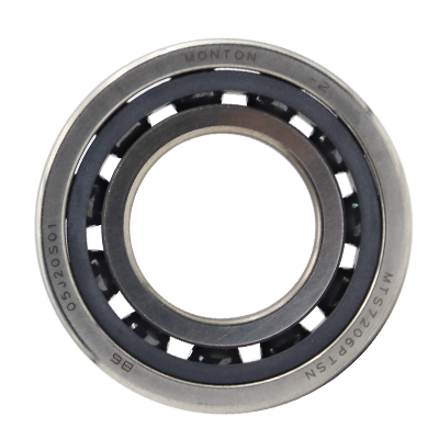
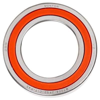
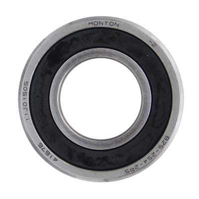
Semiconductors bearing
There has been much technological advancement in products such as Semiconductor chip, FPD (Flat Panel Display), Solar panel and Cell phone. For the Semiconductor chip, miniaturization has led to circuit linewidth design decreasing from 32 nm to 22 nm, and large scale integration allows change from single to multiple packaging design (System in Package) which accomplish lower power consumption, higher operating speed and smaller chip size. For the FPD, the panel size has been increased to 2850mm x 3050mm (10th generation) from 2500mm x 2300mm (8th generation). Due to advancement and industry trend in Semiconductor or FPD manufacturing equipment, the components such as Bearing, Linear motion products and Mechatronics products are required to obtain lower dust emission, lower out gas, higher thermal resistance, better corrosion resistance, higher rigidity, higher speed and higher accuracy.
Semiconductors bearing Application:
Inspection equipment
Wafer probers
Sputtering equipment
Wafer transfer systems
Dispensing
Pick and place robotics
Measuring systems
Test head
Positioners
Dicing equipment
Lapping equipment
Vacuum deposition systems
Wafer steppers
Probe stations
Arms
Wafer trimmers
Wafer scrubbers
Wafer polishers
Thin-film deposition systems
CVD systems
Etching systems
Mechanical polishers
Atmospheric & vacuum transfer
Robots
Test heads
Manipulators
Megasonic cleaning systems
Spin dryers
Photolithography
Mechanical polishers
Die bonders
![]()
Previous: Monton bearing official homepage